 欢迎来到上海巨纳科技有限公司网站!
 欢迎来到上海巨纳科技有限公司网站!
当前位置:首页 > 产品中心 > 196体育APP官网 > 二维材料薄膜 > 基于蓝宝石衬底的全区域覆盖的单层二硒化铼


详细介绍
This product contains full area coverage ReSe2 monolayers on c-cut sapphire substrates. Sample size measures 1cm in size and the entire sample surface contains monolayer thick ReSe2 sheet. Synthesized full area coverage monolayer ReSe2 is highly crystalline, some regions also display significant crystalline anisotropy.
Sample Properties.
Sample size | 1cm x 1cm square shaped |
Substrate type | Sapphire c-cut (0001) |
Coverage | Full monolayer coverage |
Electrical properties | 1.45 eV Anisotropic Semiconductor (Indirect Bandgap) |
Crystal structure | Distorted Tetragonal Phase (1T’) |
Unit cell parameters | a = 0.656 nm, b = 0.672 nm, c = 0.674 nm, α = 91.74°, β = 105°, γ = 119° |
Production method | Atmospheric Pressure Chemical Vapor Deposition (APCVD) |
Characterization methods | Raman, angle resolved Raman spectroscopy, photoluminescence, absorption spectroscopy TEM, EDS |
Specifications
ReSe2 monolayers do not contain intentional dopants or defects. However, our technical staff can produce defected ReSe2 using α-bombardment technique.
Supporting datasets [for 100% Full area ReSe2 monolayers on c-cut Sapphire]

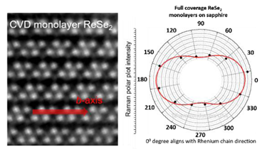
Transmission electron images (TEM) and angle resolved Raman spectroscopy measurements acquired from CVD grown full area coverage ReSe2 monolayers on c-cut sapphire confirming crystalline anisotropy

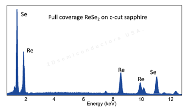
Energy dispersive X-ray spectroscopy (EDX) characterization on CVD grown full area coverage monolayer ReSe2 on c-cut sapphire

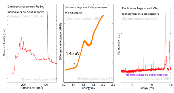
Raman spectroscopy measurement confirm monolayer nature of the CVD grown samples. Differential reflectance measurements clearly show band gap at 1.45 eV for monolayer ReS2 consistent with the existing literature values. PL spectrum does not show any PL signal due to indirect band nature.
产品咨询
联系我们
上海巨纳科技有限公司 公司地址:上海市虹口区宝山路778号海伦国际大厦5楼 技术支持:化工仪器网扫一扫 更多精彩

微信二维码

网站二维码